

Is your trouble in the details?
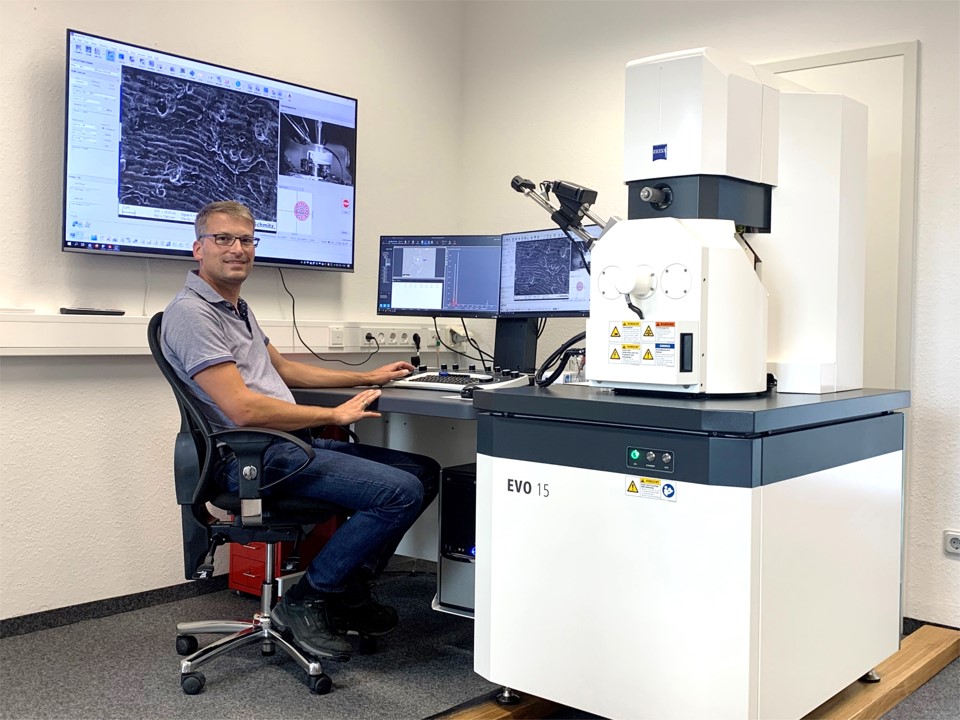
A fully equipped, modern electron microscope with EDX detector is indispensable for failure analysis.
We are happy to offer you an examination of your samples using our scanning electron microscope.
Jump to the desired topic:
- Fields of application
- Application example: Fracture surfaces
- Application example: precipitations in aluminum
- Application example: corrosion product
- Application example: chromium oxide layer
- Design and operation of a scanning electron microscope
- Sample preparation for scanning electron microscopy
- Chemical analysis by means of EDX detector
Fields of application
- Assessment of fracture surfaces, corrosion attacks or other damage mechanisms
- Chemical analysis by means of EDX detector (impurities, corrosion products, foreign matters, coatings …)
- Analysis of microstructural components or coatings in addition to light microscopy
Application example: Fracture surfaces
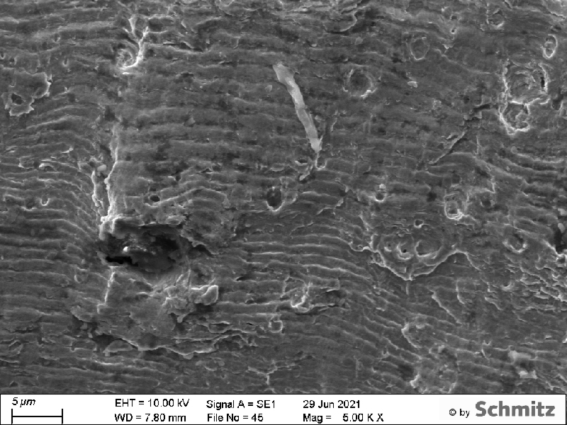
Here you can see three different types of fracture surfaces as examples: fatigue fracture (right), intergranular fracture (bottom left) and overload fracture (bottom right).
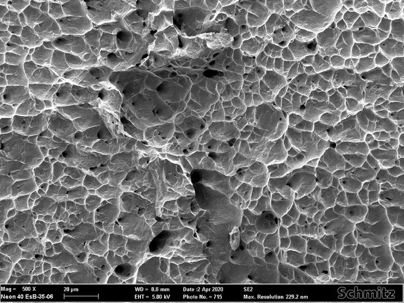
You can find more images from the SEM here
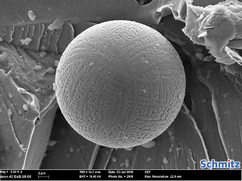
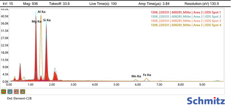
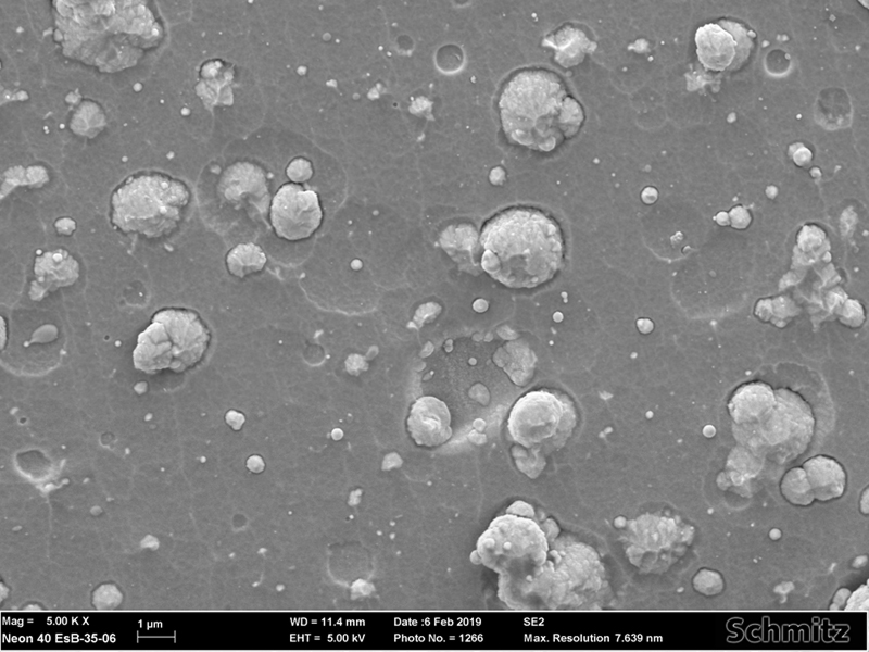
Application example: Precipitations in aluminum
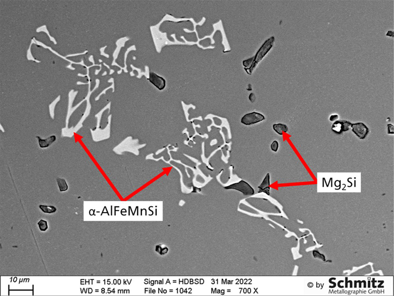
These precipitations, reminiscent of Chinese characters, in an aluminum alloy were identified using our EDX detector.
Thanks to many investigations in this field, we now have an extensive database of possible precipitation types in various aluminum alloys.
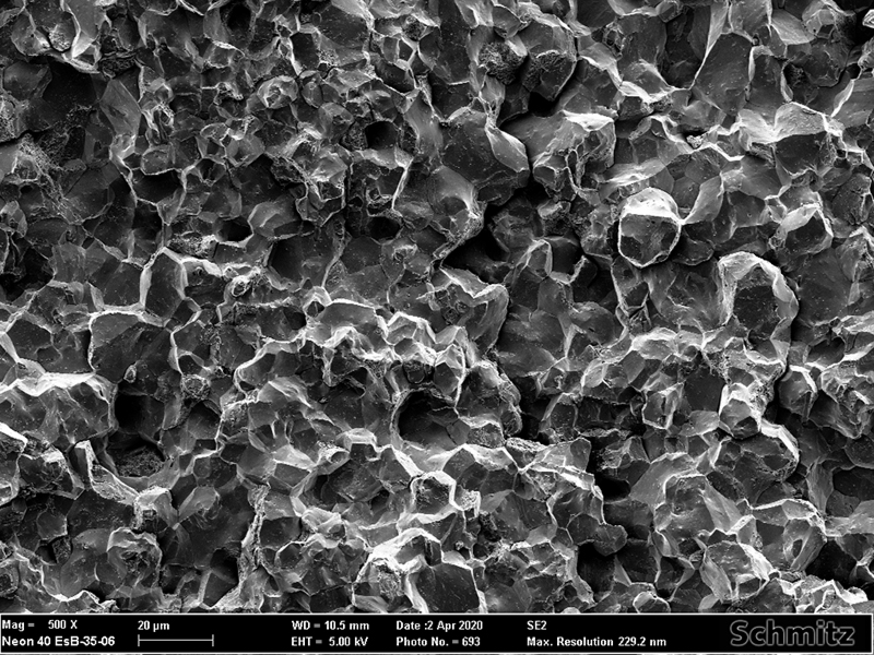
Application example: Corrosion product
The green corrosion products of shallow pitting/crevice corrosion in water mains pipes can take on bizarre shapes.
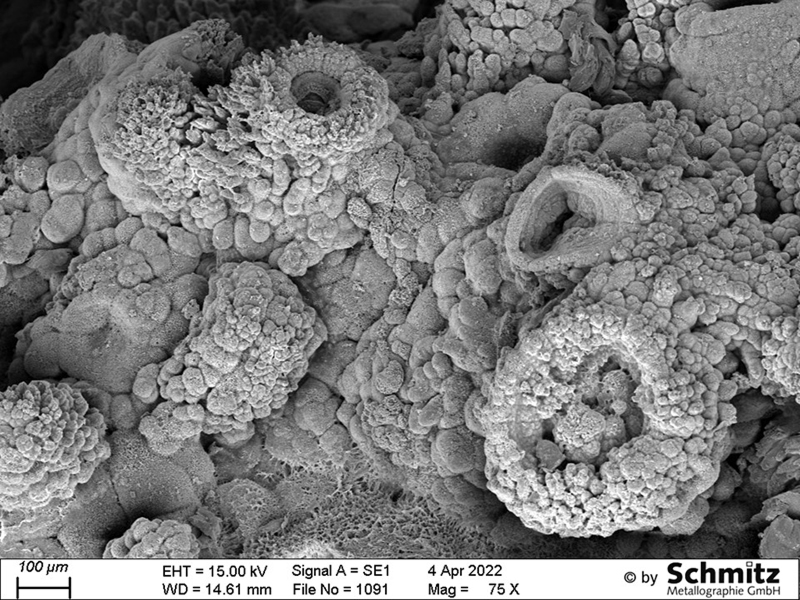
Application example: Chromium oxide layer
The chromium oxide layer contains nodular growth defects, which are typical for coatings applied by means of PVD process.
Design and operation of a scanning electron microscope
In scanning electron microscopy (SEM), a specimen is scanned by means of a finely focused electron beam in a high vacuum. Interactions of the electrons with the specimen are used to generate an image.
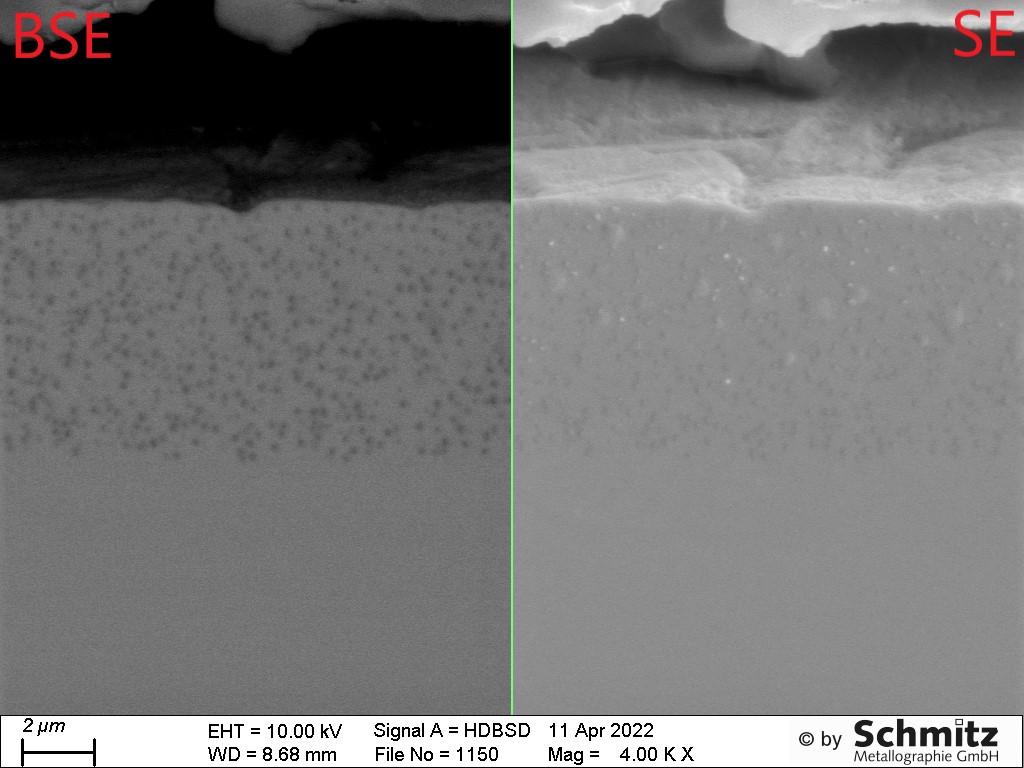
Secondary electron contrast (SE): The low-energy secondary electrons emitted from a sample by excitation with a primary electron beam originate from the uppermost nanometers and map the topography of the surface. Elevations appear bright, depressions dark.
Backscattered electron contrast (BSE): This uses the high-energy electrons backscattered from the specimen. The signal intensity depends on the atomic number of the element: The heavier an element, the brighter it appears. The BSE image therefore provides indications of, for example, inhomogeneities in the sample surface, impurities or oxidation products, which can then be identified using EDX.
The SEM examination requires a conductive surface. If necessary, the specimen is sputtered with gold for this purpose.
Sample preparation for scanning electron microscopy
The prerequisite for examining a specimen using scanning electron microscopy is both an electrically conductive specimen surface and a conductive connection between the specimen and the specimen holder. In the case of a non-conductive surface, space charges could be generated by the trapped, non-flowing electrons. These space charges interfere with the electron steel and can greatly affect the imaging due to abrupt discharges. One way to examine non-conductive samples is to use an SEM with low vacuum technology. If this is not available, the sample must be sputtered.
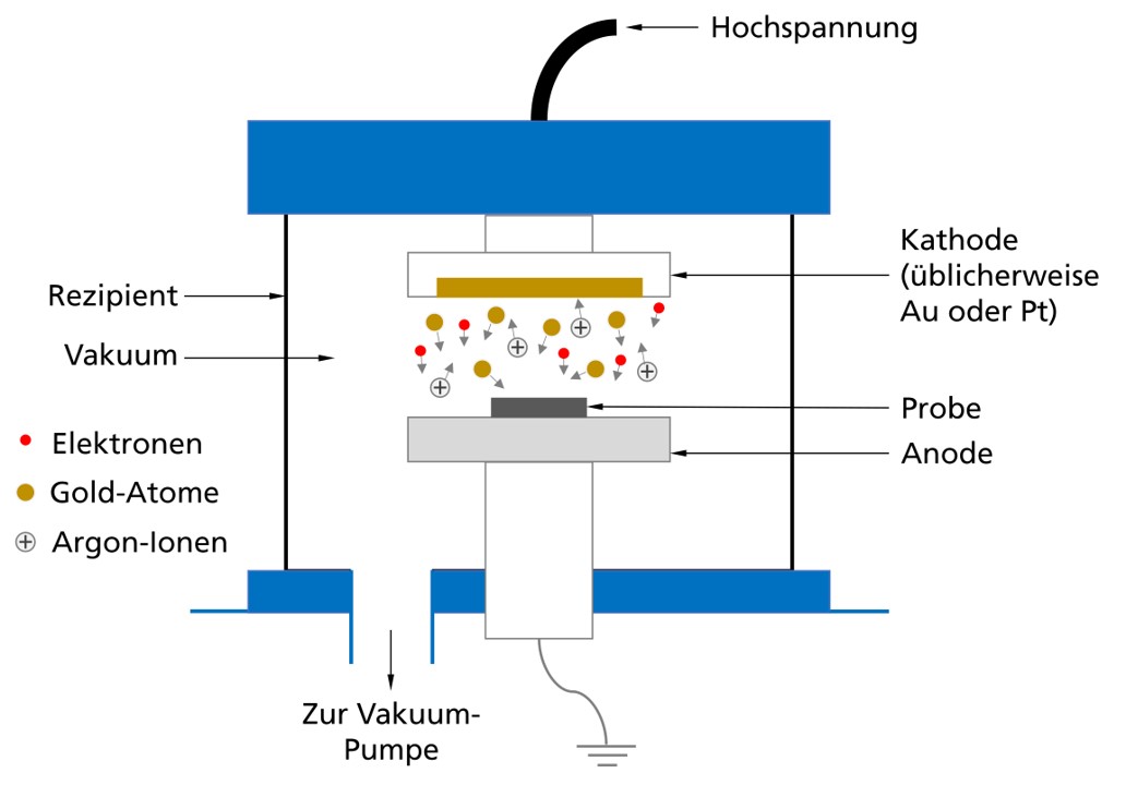
The recipient in which sputtering takes place contains both an anode and a cathode, usually made of gold or platinum. The sample is placed in this recipient. First a vacuum is applied, then an argon atmosphere. A voltage applied between the anode and cathode creates a plasma containing both argon ions and electrons. The argon ions are accelerated towards the cathode due to the voltage and knock out some gold (or platinum) atoms when they meet the cathode. These knocked out atoms move freely through the recipient and often collide on their way. As a result, they spread evenly over the sample surface and form the desired conductive gold layer. A layer thickness of approximately 20 nm is normally sufficient for examination in the SEM.
Chemical analysis by means of EDX detector
The characteristic X-ray radiation is used to characterize the local elemental composition at the sample surface. This is produced when the primary electron beam knocks out an electron from a shell closer to the nucleus in the sample. This gap is immediately filled by a higher-energy electron of a higher orbital, and the energy difference is released in the form of an X-ray quantum. This X-ray radiation is characteristic of each individual element and is detected by an EDX (energy dispersive X-ray spectroscopy) detector. Further information on the formation of X-rays can be found here. Area and point analyses, linescans and mappings of the sample surface are possible.
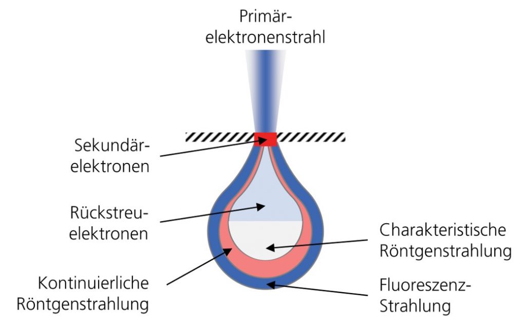
The precision of EDX analysis is limited by the fact that the emitted X-rays originate not only from the immediate surface, but from a pear-shaped volume below (“excitation pear”). This is due to a certain penetration depth of the electron beam into the sample, and the beam is also scattered in the material.